
The Shift to Optical Computing
For decades, the backbone of modern computing has relied on the movement of electrons through copper pathways. While this architecture has powered everything from calculators to the latest AI-driven supercomputers, it has hit a physical ceiling: heat generation and energy loss. As data requirements skyrocket, the inefficiency of moving electricity across microchips has become a primary bottleneck. A breakthrough from the Technical University of Denmark (DTU) aims to change this paradigm by shifting the burden from electrons to photons.
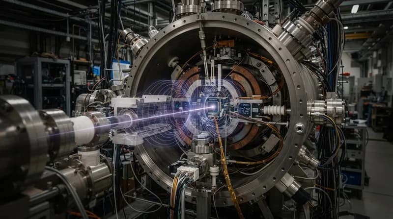
By integrating a new, ultra-small nanolaser directly onto semiconductor membranes, researchers have paved the way for chips that communicate using light. This technology mimics the long-distance efficiency of fiber optic internet cables but scales it down to the microscopic architecture of a processor. The result is a potential 50% reduction in energy consumption for high-performance computing tasks.
Breakthrough in Dielectric Confinement
The core challenge in creating on-chip lasers has historically been size. To make a laser functional, light must be trapped and concentrated in a cavity; traditionally, this required bulky components that could not fit onto the dense grid of a modern microchip. The DTU team, led by Professor Jesper Mørk and his colleagues, bypassed this constraint by utilizing a novel 'nanocavity' structure.
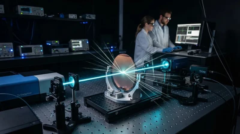
This structure, developed with assistance from Professor Ole Sigmund’s group, allows for extreme dielectric confinement. By trapping both photons and electrons within an incredibly tight space, the device functions effectively at room temperature. This level of precision was previously considered physically impossible, yet the DTU team successfully demonstrated it in a clean room environment. Because these lasers are small enough to be integrated by the thousands on a single processor, they provide a scalable solution for optical data transmission.
Why it Matters
The implications of moving from electricity to light-based data transfer are profound for the future of hardware development. Here is why this advancement is a game-changer:
- Drastic Power Efficiency: By eliminating the resistance inherent in electronic circuitry, these nanolasers could cut the energy footprint of data centers—some of the world's largest power consumers—by half.
- Thermal Management: Moving data with light generates significantly less heat than electrical impulses. This allows for higher clock speeds without the need for aggressive cooling solutions.
- Medical and Sensing Applications: The extreme light concentration of these nanolasers enables the development of high-resolution biosensors, which could lead to breakthroughs in medical imaging and non-invasive diagnostic tools.
- Compact Hardware: Because these lasers are built directly into semiconductor membranes, they can eventually be integrated into existing fabrication processes for smartphones and portable electronics.
Looking Toward Commercialization
While the laboratory success of this nanolaser is a milestone, the team acknowledges that the path to a consumer-ready chip involves further refinement. The primary hurdle currently facing researchers is the transition from light-pumped operation to electrical-current operation. If the team can successfully drive these nanolasers using standard electronic currents, it would effectively complete the integration process for modern silicon-based hardware.
Researchers estimate that these remaining technical challenges could be resolved within the next five to ten years. As the industry looks for ways to push past the limits of traditional transistors, light-based communication may be the key to the next generation of high-performance, energy-conscious hardware. This leap in nanophotonics ensures that the future of computing will be not just faster, but significantly more sustainable.