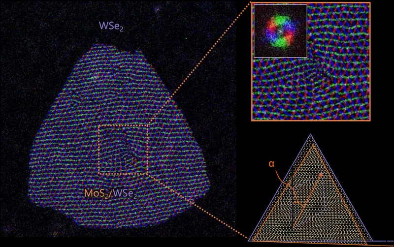
Recent research published in Physics World has provided new clarity on the mechanisms of strain relaxation within van der Waals (vdW) heterostructures. These materials, composed of atomically thin layers held together by weak intermolecular forces, are essential for the next generation of nanoelectronics and optoelectronics.
Managing Lattice Mismatch
When different two-dimensional materials are stacked, the differences in their atomic lattice constants often create mechanical strain. Unlike traditional covalently bonded semiconductors, vdW heterostructures handle this mismatch through unique relaxation processes at the nanoscale. Understanding these processes is critical for maintaining the electronic properties and structural integrity of the devices.
The findings suggest that the way these layers shift and adjust can be precisely controlled, offering a new toolkit for materials scientists to engineer properties such as bandgap and carrier mobility. This development marks a significant step forward in the reliable manufacturing of heterostructure-based technology.