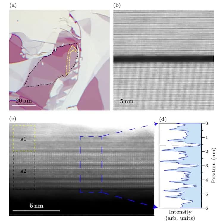
A breakthrough in materials science has allowed researchers to visualize the surface structure of 2D quantum materials with unprecedented clarity. By utilizing a new encapsulation technique, scientists can now protect and probe the top layer of atomically thin topological materials, a task that was previously hindered by environmental degradation and technical limitations.
Probing the Atomic Frontier
Topological quantum materials are of high interest due to their unique electronic properties, which could revolutionize future computing and sensor technologies. However, because these materials are often only one or a few atoms thick, their surfaces are incredibly sensitive. Traditional imaging methods often struggle to capture the delicate surface states without damaging the sample.
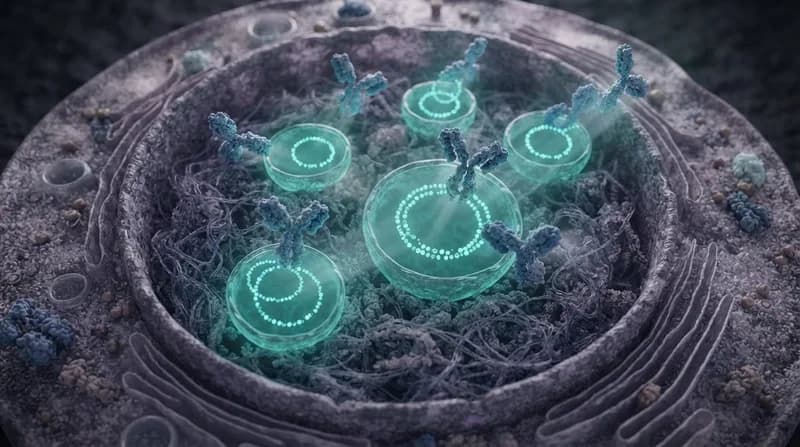
The encapsulation process acts as a protective shield, stabilizing the material while allowing advanced imaging tools to bypass interference. This allows for the first-ever direct observation of the top-most layer's structural characteristics, providing essential data for developing next-generation quantum devices.