
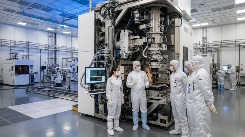
The Shift Toward 12-Inch Photomasks
In a major strategic shift for the semiconductor industry, ASML and TSMC have unveiled a collaborative initiative to transition toward 12-inch photomasks for extreme ultraviolet (EUV) lithography. While current high-NA EUV systems rely on the industry-standard 6-inch format, the push for larger masks is being driven by the need to increase manufacturing productivity and eliminate the technical hurdles inherent in advanced process nodes. The initiative has already garnered significant backing from major industry players, including Intel Foundry and Samsung Electronics, signaling a unified roadmap toward full-scale integration.
The move to 12-inch masks is comparable in scale to the industry’s historic transition from 200mm to 300mm wafers. ASML aims to establish a functional 12-inch mask pilot line by 2031, with the goal of having the corresponding lithography systems ready for high-volume, advanced-node production by 2033. By broadening the surface area of the photomask, the industry aims to bypass the limitations currently imposed by anamorphic optical designs.
Solving the Stitching Dilemma
The current generation of high-NA EUV machinery utilizes an anamorphic optical design that reduces image projection by 4x in one axis and 8x in the other. This compromise was necessary to allow manufacturers to continue using existing 6-inch masks, but it resulted in an exposure field exactly half the size of previous machines. For the increasingly large, high-performance dies required for AI and specialized compute applications, this restricted field size necessitates "stitching"—a process where two separate exposure patterns must be aligned perfectly to form a single chip.
Stitching adds significant manufacturing complexity, slows down throughput, and introduces potential yield risks. By transitioning to 12-inch masks, chipmakers will be able to restore the full exposure field. This enables larger, more complex monolithic designs to be manufactured in a single pass, drastically improving the efficiency and energy profile of future processors. As transistor architectures grow more complex to satisfy the insatiable demands of the AI era, this restoration of the exposure field is becoming a non-negotiable requirement for the leading edge of semiconductor scaling.
Why It Matters
- Enhanced Productivity: Eliminating stitching processes reduces manufacturing complexity and increases overall wafer throughput.
- Scalability: Larger masks provide the necessary surface area for massive, next-generation AI-accelerator dies that would otherwise exceed current high-NA EUV field limits.
- Industry Alignment: The collaboration between ASML, TSMC, Intel, and Samsung ensures a standardized supply chain, which is critical for the capital-intensive transition of lithography tooling.
- Future-Proofing: This development prepares the foundation for post-2nm nodes, ensuring that chipmakers have the physical infrastructure to continue shrinking transistors without hitting a wall in optical performance.
A New Era of Semiconductor Manufacturing
The transition is not merely a hardware upgrade; it is a fundamental reconfiguration of the semiconductor value chain. Samsung Electronics has already signaled its intent to leverage ASML’s high-NA technology for high-volume DRAM production as early as 2028, highlighting that these advancements will impact memory as much as logic processors. As the AI era continues to drive the demand for more efficient and faster chips, the alignment of toolmakers, mask suppliers, and fab operators becomes the single most important factor in maintaining Moore’s Law.
While the industry will continue to utilize 6-inch masks for the initial rollout of high-NA EUV, the long-term roadmap clearly favors the 12-inch format. By aligning early on these standards, the major foundry players are ensuring that when the 2033 target for full production arrives, the manufacturing ecosystem will be fully equipped to handle the next generation of semiconductor innovation.